Author Affiliations
Abstract
1 School of Nano-Tech and Nano-Bionics, University of Science and Technology of China, Hefei 230026, China
2 Suzhou Institute of Nano-Tech and Nano-Bionics, Chinese Academy of Sciences, Suzhou 215123, China
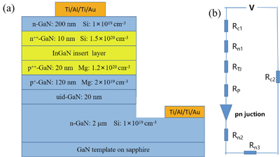
The InGaN films and GaN/InGaN/GaN tunnel junctions (TJs) were grown on GaN templates with plasma-assisted molecular beam epitaxy. As the In content increases, the quality of InGaN films grown on GaN templates decreases and the surface roughness of the samples increases. V-pits and trench defects were not found in the AFM images. p++-GaN/InGaN/n++-GaN TJs were investigated for various In content, InGaN thicknesses and doping concentration in the InGaN insert layer. The InGaN insert layer can promote good interband tunneling in GaN/InGaN/GaN TJ and significantly reduce operating voltage when doping is sufficiently high. The current density increases with increasing In content for the 3 nm InGaN insert layer, which is achieved by reducing the depletion zone width and the height of the potential barrier. At a forward current density of 500 A/cm2, the measured voltage was 4.31 V and the differential resistance was measured to be 3.75 × 10?3 Ω·cm2 for the device with a 3 nm p++-In0.35Ga0.65N insert layer. When the thickness of the In0.35Ga0.65N layer is closer to the “balanced” thickness, the TJ current density is higher. If the thickness is too high or too low, the width of the depletion zone will increase and the current density will decrease. The undoped InGaN layer has a better performance than n-type doping in the TJ. Polarization-engineered tunnel junctions can enhance the functionality and performance of electronic and optoelectronic devices.
GaN/InGaN/GaN tunnel junctions polarization-engineering molecular beam epitaxy Journal of Semiconductors
2024, 45(1): 012503

Author Affiliations
Abstract
1 Key Laboratory of Nanodevices and Applications, Suzhou Institute of Nano-Tech and Nano-Bionics, Chinese Academy of Sciences, Suzhou 215123, China
2 Nano Science and Technology Institute, University of Science and Technology of China, Suzhou 215123, China
3 Vacuum Interconnected Nanotech Workstation (NANO-X), Suzhou Institute of Nano-Tech and Nano-Bionics, Chinese Academy of Sciences, Suzhou 215123, China
The atomic structure and surface chemistry of GaP/Si(100) heterostructure with different pre-layers grown by molecular beam epitaxy are studied. It is found that GaP epilayer with Ga-riched pre-layers on Si(100) substrate has regular surface morphology and stoichiometric abrupt heterointerfaces from atomic force microscopes (AFMs) and spherical aberration-corrected transmission electron microscopes (ACTEMs). The interfacial dynamics of GaP/Si(100) heterostructure is investigated by X-ray photoelectron spectroscopy (XPS) equipped with an Ar gas cluster ion beam, indicating that Ga pre-layers can lower the interface formation energy and the bond that is formed is more stable. These results suggest that Ga-riched pre-layers are more conducive to the GaP nucleation as well as the epitaxial growth of GaP material on Si(100) substrate.The atomic structure and surface chemistry of GaP/Si(100) heterostructure with different pre-layers grown by molecular beam epitaxy are studied. It is found that GaP epilayer with Ga-riched pre-layers on Si(100) substrate has regular surface morphology and stoichiometric abrupt heterointerfaces from atomic force microscopes (AFMs) and spherical aberration-corrected transmission electron microscopes (ACTEMs). The interfacial dynamics of GaP/Si(100) heterostructure is investigated by X-ray photoelectron spectroscopy (XPS) equipped with an Ar gas cluster ion beam, indicating that Ga pre-layers can lower the interface formation energy and the bond that is formed is more stable. These results suggest that Ga-riched pre-layers are more conducive to the GaP nucleation as well as the epitaxial growth of GaP material on Si(100) substrate.
Journal of Semiconductors
2022, 43(12): 122101
1 上海大学 材料科学与工程学院, 上海 200444
2 中国科学院苏州纳米技术与纳米仿生研究所 中国科学院纳米器件与应用重点实验室, 江苏 苏州 215123
3 上海空间电源研究所 光伏研究中心, 上海 200245
对柔性GaAs基太阳电池的制备方法进行研究, 报道了一种用于制备柔性倒置生长的AlGaInP/AlGaAs/GaAs三结太阳电池的剥离和转移方法——金属背支撑选择性湿法刻蚀技术。在GaAs/GaInP选择性腐蚀的基础上进行了GaAs衬底层的腐蚀, 研究了不同类型和体积比的溶液对GaAs/GaInP/AlInP结构腐蚀的选择特性, 最终选用不同配比的H2SO4-H2O2系腐蚀液, 获得快速、可控制、重复性好的去除衬底的两步腐蚀法。原子力显微镜测试结果表明, 通过此方法能够成功地将电池外延层薄膜转移到Cu衬底上, 并且在剥离和转移过程中外延层薄膜没有受到损伤。柔性AlGaInP/AlGaAs/GaAs三结太阳电池的开路电压超过3.4V。
太阳电池 柔性薄膜 湿法腐蚀 重量比功率 AlGaInP/AlGaAs/GaAs AlGaInP/AlGaAs/GaAs solar cell flexible film wet etching power-to-weight ratio


